Cybertruck Power Electronics

Crissa

Well-known member
First Name
Crissa
Joined
Jul 8, 2020
Threads
127
Messages
16,612
Reaction score
27,659
Location
Santa Cruz
Vehicles
2014 Zero S, 2013 Mazda 3
Country flag
I think they're wrong about it not working for 3D layere chips - just that it'll be more difficult and perhaps even more important.

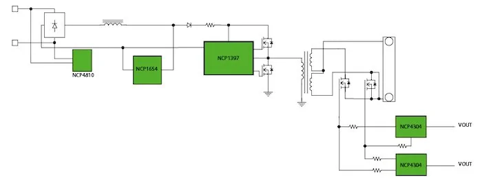
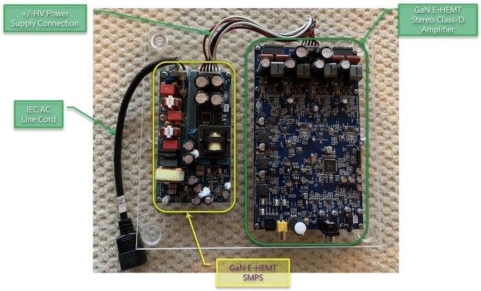
But power electronics get so hot that they burn out really commonly, and that's limiting the ability to shrink them.

-Crissa
Sponsored


lqdchkn

Well-known member
First Name
B
Joined
Sep 15, 2020
Threads
1
Messages
78
Reaction score
78
Location
TX
Vehicles
CT
Country flag
So I skimmed most of this and aside from the first article all of this seems to just be generic electrical component tech and nothing specific to any particular component in the Cybertruck or anything specific that Tesla uses, does.

Where's the association?
 
OP
OP
TruckElectric

TruckElectric

Well-known member
First Name
Bryan
Joined
Jun 16, 2020
Threads
769
Messages
2,482
Reaction score
3,273
Location
Texas
Vehicles
Dodge Ram diesel
Occupation
Retired
Country flag
Mersen Fischerlink’s low-inductance busbar/capacitor assembly for SiC DC-link

Tesla Cybertruck Cybertruck Power Electronics FischerLink-image


Optimized and Compact Design

Mersen Fischerlink 2.0 is an optimally designed and assembled capacitor and bus bar sub assembly. Traditionally capacitors are connected to bus bars by screw or solder connections which may cause increased inductance in the sub-assembly. Mersen Fischerlink 2.0 uses laser welding to connect capacitor terminals to bus bars, thus improving the overall performance of the assembly and reducing the footprint.
Laser welding the connections has several advantages compared to traditional screw or solder mounting methods. Laser welding reduces the inductance and increases capacitance. Additionally the capacitance per volume can be increased up to 20%. Since the assembly is done by Mersen, all parts are 100% tested before delivery providing customer an additional degree of peace of mind. The sub-assembly of capacitor and bus bar rolled into one single part number offers additional savings in administrative costs.

Design Performance Comparison Example

Tesla Cybertruck Cybertruck Power Electronics rLink-Design-Performance-Comparison-Example-Mersen


SOURCE: MERSEN
 
OP
OP
TruckElectric

TruckElectric

Well-known member
First Name
Bryan
Joined
Jun 16, 2020
Threads
769
Messages
2,482
Reaction score
3,273
Location
Texas
Vehicles
Dodge Ram diesel
Occupation
Retired
Country flag
VisIC unveils new 8mOhm power switch for EV Inverters


Designed for EV, the high power D3GaN 8mOhm product for high voltage and high current Inverter applications brings higher efficiency and smaller size

- Low Ron power GaN switch based on D3GaN technology for the EV market

- The new solution designed specifically for the EV Inverter application

NESS ZIONA, Israel, Dec. 16, 2020 /PRNewswire/ -- VisIC Technologies Ltd., a global leader in gallium nitride (GaN) devices for automotive high-voltage applications, is proud to announce its new low resistance product for EV Inverter application that will improve efficiency and manufacturing cost of electric cars. The new 8mOhm product is another step in the ongoing effort to support our customers and improve the power conversion systems.


Tesla Cybertruck Cybertruck Power Electronics Screen Shot 2020-12-17 at 1.50.17 PM

"The V8 product doubles the current capabilities and reduces resistance by a factor of 2.5 times over the previous generation of VisIC product. This will allow our customers to improve their inverter systems to be more efficient in size, power, and cost for the target EV market." said Mr. Ran Soffer, VisIC SVP Sales & Marketing. "The V8 product is another step in our long-term effort to provide a better solution based on our D3GaN technology. The work on the new product is done in close collaboration with our leading customers to bring meaningful improvement to the electric drive system which is the heart of the Electrical Vehicle. The higher power density can also be achieved in high-power traction invertors", added Mr. Ran Soffer.


The new product is rated at 8mΩ, 650V, 200Amp and provides significantly lower switching losses versus comparable IGBT or SiC devices for the same current range. Customers can integrate the new die into both discrete packages and power modules with a variety of interconnect options. This new technology enables power loss savings particularly in drive cycle tests for high current Electric Vehicle inverter systems.

The challenge of manufacturing a single die with a high current is a known challenge for wide band gap technologies (WBG), such as SiC and GaN, vs ubiquitous Silicon dies. The breakthrough of 200A GaN dies has been made possible due to the thoughtful design of the D3GaN platform and manufacturing excellence of TSMC, the manufacturing partner of VisIC company. This breakthrough will enable Electric Vehicles to benefit from the high-efficiency technology of GaN. This will lead to more cost-effective EV cars, for a greener and cleaner planet.

This press release and further information can be found at www.visic-tech.com

SOURCE: PRNEWSWIRE
 
OP
OP
TruckElectric

TruckElectric

Well-known member
First Name
Bryan
Joined
Jun 16, 2020
Threads
769
Messages
2,482
Reaction score
3,273
Location
Texas
Vehicles
Dodge Ram diesel
Occupation
Retired
Country flag
“GaN Is Like a Ferrari:” How GaN Is on the Fast Track for 2021
by Jake Hertz

2020 ushered in a wave of GaN transistors in applications from automobiles to audio amplifiers. We talked with GaN Systems CEO Jim Witham to find out why he thinks 2021 could see even more GaN adoption.

While gallium nitride (GaN) transistors were once the musings of university research projects 20 years ago, these devices are now widely adopted across the industry—especially in 2020.

GaN transistors are now a popular substitute for silicon-based FETs because they offer extremely high electron mobility. This also gives GaN a leg up with smaller on-resistances and significantly faster switching speeds than silicon-based transistors.


Tesla Cybertruck Cybertruck Power Electronics GaN_vs._Si_transistors_


GaN transistors are driven in the same way as conventional MOSFETs, making them easy to integrate into existing designs. This is partly why 2020 marked a market high of GaN acceptance with more power supplies, audio amplifiers, data centers, and automotive systems implementing GaN than ever before.


Tesla Cybertruck Cybertruck Power Electronics for_GaN_power_transistors_have_skyrocketed_in_2020

The market opportunities for GaN power transistors have skyrocketed in 2020. Image used courtesy of GaN Systems

All About Circuits had the privilege of speaking with Jim Witham, the CEO of GaN Systems, (who we also interviewed back in 2018) to hear his predictions on the future of GaN and why 2021 might push this technology even further into ubiquity.


Medium Voltages: GaN's Sweet Spot

To begin, it seems that GaN has hit its stride in a number of key industries, from fast chargers to data centers. While GaN isn't the solution to every power application, its "sweet spot," according to Witham falls in the 60 V to 1200 V range.

"Silicon works for low voltages (60 V and below) and low power, GaN is ideal for medium voltages (60–1200 V) and medium power, and SiC and IGBTs suit high voltages (1200 V and above) and high power," he observes.


Chargers and Adapters

One market that saw widespread GaN adoption in 2020 was the charger and adapter market for applications like phones, tablets, and handheld gaming devices.

An immediate reason for this demand was the widespread push for fast charging, particularly from Asia-based manufacturers. Faster charging requires higher power levels, which often means bulkier equipment. GaN fills this market need with smaller chargers and higher power levels.


Tesla Cybertruck Cybertruck Power Electronics _ON_Semiconductors_GaN-enabled%C2%A0power_supplies


Block diagram of one of ON Semiconductor's GaN-enabled power supplies. Image used courtesy of ON Semiconductor


“In particular, Huawei, Oppo, and Xiaomi are all really pushing fast charge," says Witham. GaN Systems predicts that 2021 will see other big-name brands start to bring their own GaN chargers to market, too, as GaN becomes an industry standard.


Audio

During our conversation, Witham recounted his experience in a "sound off" between a silicon amplifier and a GaN amplifier. At first, he was concerned the difference wouldn't be notable. "Man, it is so easy [to hear the difference]," he remarked. "You close your eyes and you think you're hearing a live concert."

Growing demand for small, high-quality audio devices at low power has made the Class D audio amplifier a fan favorite for designers. Relying on a MOSFET output stage, the Class D amplifier relies on the fast switching speed of these transistors to accurately recreate the audio waveforms.


Tesla Cybertruck Cybertruck Power Electronics A_complete_audio_amplifier_platform

A complete audio amplifier platform. Image used courtesy of GaN Systems


This is another place where GaN outpaces silicon thanks to its extremely high switching speeds, sometimes up to 1,000 times faster than silicon-based FETs. A whitepaper from GaN Systems quantifies this superior audio quality, showing that a GaN-based Class D amplifier can produce a total harmonic distortion (THD) as low as 0.004% compared to 0.015% for a silicon product.

Witham comments, “I have audio guys tell me, ‘You're as close to the perfect transistor as I think we'll ever get.’” Because of decreased size and superior audio quality, GaN Systems predicts that a significant number of the world’s noteworthy audio brands will be producing GaN-based amplifiers in the coming year.


Data Centers

From GaN Systems’ perspective, GaN is a must-have fortifying pillar for increasingly overburdened data centers, which are managing unprecedented power consumption and data density as more people work from home. The company says GaN transistors can make marked improvements in three key areas:

  • AC-DC power supply, where high voltage enters server racks and must be stepped down to distribute power to all of the servers
  • DC-DC converters on the server board itself, taking the voltage from a DC voltage—whether it's 12, V, 24 V, or 48 V—down to a low chip-level voltage
  • Backup power in the event of a main power blackout


Tesla Cybertruck Cybertruck Power Electronics IMS3

GaN Systems recently announced an insulated metal substrate (IMS3) platform to be used with the company's GaN E-HEMTs in data centers. Image used courtesy of GaN Systems

Achieving smaller and more efficient power supplies will allow data centers to put more servers into their racks, increasing performance per square meter.


Automotive

The final sector in which GaN Systems sees great promise is in the automotive industry. Last year, in fact, an "all-GaN" vehicle was announced at the Toyota Motor Show. With international governments and the public increasingly demanding electric vehicles, designers are tasked with integrating smaller and more power-dense systems in addition to advanced battery technology.


Tesla Cybertruck Cybertruck Power Electronics C2%A0technology%C2%A0allows_laser_signals_in_LiDAR

Compared to silicon MOSFETs, GaN-based technology allows laser signals in LiDAR to be fired at significantly higher speeds. Image used courtesy of EPC

We recently discussed the challenges of establishing a universal reliability standard for GaN HEMTs, and GaN Systems seems attuned to this need to verify GaN safety on the road. This year, the company released its AutoQual+ program, which extends the testing sequences of AEC-Q.

In Witham’s eyes, 2021 is “all about seeing the GaN transistor on the road.”


On GaN's Cost, Design, and "Green" Values

According to GaN Systems and many other semiconductor manufacturers, the early concerns surrounding GaN are no longer looming.

"GaN saves money above a kilowatt. As volumes go up, costs go down," Witham says. Beyond price, though, suppliers provide robust technical documentation—white papers, application notes, reference designs, and more—to support designers who are still adjusting to such a fast MOSFET.

Speaking of the design learning curve, Witham observes in good humor, "GaN is kind of like a Ferrari; you've got to learn how to drive it."


Tesla Cybertruck Cybertruck Power Electronics half-bridge_compared_to%C2%A0a_GaN_FET_half-bridge

Conventional high-voltage half-bridge compared to a GaN FET half-bridge. Image used courtesy of Nexperia


One of the most exciting promises of GaN for Witham is the long-standing environmental impacts it will have. Witham concluded the conversation, saying, “We're in the midst of a power revolution. We're seeing these small, lightweight, very efficient power electronics coming out . . . [and] they'll make the planet a better place.”

GaN Systems sees gallium nitride as the basic building block to accomplish the task.


SOURCE: ALL ABOUT CIRCUITS
 
OP
OP
TruckElectric

TruckElectric

Well-known member
First Name
Bryan
Joined
Jun 16, 2020
Threads
769
Messages
2,482
Reaction score
3,273
Location
Texas
Vehicles
Dodge Ram diesel
Occupation
Retired
Country flag
Isolation technologies for EV power electronics
Posted February 2, 2021 by Jeffrey Jenkins & filed under Features, Tech Features.

Tesla Cybertruck Cybertruck Power Electronics isolation-tech-2-scaled

A previous article on bidirectional chargers touched on using transformers to provide isolation at high power levels—in which application they are the only game in town, really—but this time the focus will be on achieving isolation at low power levels, such as the feedback signal in a regulator, data communication buses between devices, gate drivers and the like. While discrete transformers can also be used at the signal level, isolators based on optical, magnetic and capacitive technologies are far more popular, because they tend to be both lower in cost and easier to use (usually, anyway).

Tesla Cybertruck Cybertruck Power Electronics Screen Shot 2021-02-05 at 3.31.07 PM

Tesla Cybertruck Cybertruck Power Electronics Screen Shot 2021-02-05 at 3.31.39 PM


Of course, the cheapest (though not necessarily the easiest to use) option is not to use an isolator at all, so the first consideration is whether one is even necessary, either for the circuit to operate, for safety, and/or to minimize electrical noise problems. Any power converter for EV applications (charger, inverter, DC/DC converter, etc) that is either supplied by the mains or a >48 V battery pack will pretty much require strict isolation between its power (high-voltage) and control (low-voltage) circuits. In cases where isolation isn’t required for safety reasons, it still might make the circuit more reliable to use it, such as driving the gates of the switches in a totem-pole or bridge circuit. For example, to turn on a MOSFET or IGBT, its gate needs to be made more positive than its source or emitter, respectively, by about 10 V. The lower switches in a half-bridge all have their sources/emitters referred to “ground” (more correctly, the negative rail), which makes it easy to control them directly, and with little worry that noise from rapid voltage swings (i.e. high dV/dt) will be coupled back through them. The sources/emitters in the upper switches, however, do swing violently with each state change, and their potential with respect to the negative rail is undefined when off, and not even fixed when on, since the voltage across the load will vary as well (due to, say, the back EMF of a traction motor changing with RPM). To drive the upper switches requires either an isolator or a level-translating (aka “high-side”) driver IC. The latter IC essentially lets the driver for the high-side gate follow the potential of the source/emitter of the switch being driven while level-translating the control signal up to that same potential. These high-side driver ICs are enormously popular in, shall we say, cost-sensitive power supply applications, because they are much cheaper than any form of isolator and at least appear to be much easier to use. However, because there is no galvanic isolation, the swings in voltage at each transition of the source/emitter can be coupled back through them, wreaking havoc elsewhere, or even leading to an invariably fatal failure mode called “latchup,” in which the polarity of the supply terminals is effectively reversed during the high dV/dt event. An isolated gate driver IC also follows the potential on the source/emitter of the switch it is driving, but with only a small amount of parasitic capacitance to couple dV/dt back through it (and no possibility of inadvertently forward-biasing any substrate diodes, leading to latchup), it can tolerate way higher levels of dV/dt, and can be designed to withstand an almost arbitrarily high voltage as well.

Any power converter for EV applications (charger, inverter, DC/DC converter, etc) that is either supplied by the mains or a >48 V battery pack will pretty much require strict isolation between its power and control circuits.
Another common application in which isolation might not be needed for functionality, but which safety regulations may demand anyway, is the voltage (or current) feedback path in a power supply, charger, etc. If the control circuit is on the primary side of the converter’s isolation transformer, then some means of isolating the feedback signal will be necessary to maintain galvanic isolation between the primary and secondary. In some cases, the control circuit can be placed on the secondary side, however, in which case it will receive the feedback signal directly, and the burden for maintaining galvanic isolation—if necessary—will shift to the drive signals for the primary-side switches. Whether placing the control circuit on the secondary side is even possible depends entirely on how it will receive power to start working in the first place (a classic chicken-and-egg kind of problem, then). In any event—not to point out the obvious—isolation of an analog signal requires either a linear isolator or encoding/decoding of the signal so that a digital isolator can be used. As we’ll discuss next, pretty much all isolators can handle digital signals (i.e. pulses), but only the optical types have ever been used for conveying analog signals (ignoring, for the moment, isolator ICs that have the encoding/decoding circuits built into them).

Another common application in which isolation might not be needed for functionality, but which safety regulations may demand anyway, is the voltage (or current) feedback path in a power supply, charger, etc.
Optical isolators (also known by the unsurprising portmanteau optoisolators) are one of the oldest types (along with transformers) and employ many different approaches. One of the earliest examples literally consisted of an opaque tube with an incandescent lamp at one end and a photoresistive cell (usually based on CdS, or cadmium sulfide) at the other. Bandwidth was in the low single-Hz range, and linearity was terrible too, since neither the lamp nor the photoresistor are all that linear in the first place. The next major iteration replaced the incandescent lamp with an LED, and the CdS cell with a phototransistor (or photodiode), greatly improving bandwidth (a few kHz was now possible), and with better, though not exactly spectacular, linearity. Within a couple of years, it was learned that the brightness of LEDs declines over time, even when supplied by a fixed current, so these miracle light sources that were supposed to last for eternity turned out to have a finite lifespan after all. This is not as big a problem as it might seem, however, since in most applications the optoisolator is either operated digitally (that is, on or off) or else wrapped inside a feedback loop, so that the loss of brightness over time is compensated for automatically (up until the circuit runs out of loop gain or drive current, anyway). I’ve used devices based on this approach (e.g. HCNR200, LOC111, IL300) for monitoring bus voltage, and they work exceptionally well, and as long as the LED isn’t run at too high a current (losing some of the dynamic range) the operational lifespan should be >100,000 hours.

Optical isolators (also known by the unsurprising portmanteau optoisolators) are one of the oldest types (along with transformers) and employ many different approaches.
Still, even a 100,000-hour lifespan only amounts to a bit over 11 years if the product is operated 24/7, so designers sought out alternatives that didn’t rely on LEDs. The two most viable types were capacitive and micromagnetic (chip-scale transformers, basically). Capacitive isolators consist of a pair of capacitors formed by depositing a metal onto either side of a thin insulating layer (usually SiO2—the same as used in CMOS ICs), with one capacitor carrying AC in the forward direction and the other carrying the return current. The insulating layer forms a contiguous barrier which does not rely on an air gap at all (unlike the typical optoisolator), so it can meet stringent safety regulations on creepage and clearance distances within a relatively small package. Since the capacitances involved here are extremely small, signals are usually encoded by either having them modulate the frequency of a much higher-frequency oscillator (i.e. FM) or toggling said oscillator on and off (i.e. burst AM); the former could be used for conveying analog signals, while the latter is strictly for digital applications (including gate drivers). The main downside to capacitive isolators is that they tend to have relatively poor immunity to noise coupled across them as a result of high dV/dt—Common Mode Transient Immunity, or CMTI, is the key spec to look for in the datasheet. Devices intended for gate-driver use will have appropriately high levels of CMTI, but caveat emptor if one tries to use a garden-variety digital capacitive isolator as a gate driver.

Since making the insulator thicker doesn’t really affect the magnetic operation, it’s easier to achieve an almost arbitrarily high voltage withstand rating than it is with the capacitive type.
Isolators based on magnetic coupling consist of tiny spiral coils of metal printed onto either side of an insulator (again, usually SiO2, though polymeric materials are used as well). The magnetic field from one coil induces a current in the other, just like a regular transformer, and since making the insulator thicker doesn’t really affect the operation—just slightly lowering the coupling coefficient with increasing distance between the coils—it’s easier to achieve an almost arbitrarily high voltage withstand rating than it is with the capacitive type. These micro-sized transformers can also be used to provide isolated power to the secondary side circuitry, which is a huge advantage over pretty much every other isolator technology (save using actual gate-drive transformers). Theoretically, magnetic isolators are susceptible to bit-flipping or other erroneous operation from external magnetic fields, but in practice this rarely seems to be an issue, because the coils are so small that they really only respond to very high frequencies. The main downsides to magnetic isolators are that they tend to consume more power for a given data rate than capacitive types (though perhaps not any more than traditional optoisolators) and that they usually cost a lot more than capacitive types because of the more complicated fabrication process (though, again, on par with the cost of equivalent optoisolators).

The last type of isolator to be discussed here is the one mentioned first: a discrete, signal-level transformer. These are constructed much like their higher-power brethren, but with perhaps more emphasis on minimizing the number of turns at the expense of a larger core size (to reduce leakage inductance and stray capacitance). While signal transformers are widely used in data isolators—every Ethernet port on the planet has one, for example—they are also quite popular in gate-drive applications because they convey the power needed to slew the gate directly from the driver circuit itself. Another advantage is that additional switches can be driven by merely adding more secondaries. It would seem, then, that a transformer is the simplest way to drive the gates of any high-side switches, but there are a number of gotchas waiting to trap the unwary. One of the most insidious is that leakage inductance—which arises from the less-than-perfect coupling between windings in a transformer—opposes each change in voltage by creating a small spike and by looking like a high impedance. The latter results in the driver circuit being effectively disconnected from the gate until the leakage inductances are reset, which can lead to spurious operation of the switch, and even short bursts of oscillation (the old and colorful term for such is snivet), both of which can cause the switch to fail (or the product to fail EMC compliance testing). Another downside to transformers is that the forward and reverse volt * seconds must be equal to prevent core saturation. This means that a unipolar signal (such as from 5 V logic) must first be converted to bipolar with an average value of 0 V, and the simplest way to do that is with a coupling capacitor. This approach is best suited for cases in which a rather narrow range of duty cycle needs to be accommodated, which means it isn’t a good choice for motor drives, buck converters, and the like. Otherwise, IC isolators using either capacitive or micromagnetic technology have proven to be superior overall, not only to transformers but to their optical predecessors as well.


This article appeared in Charged Issue 52 – November/December 2020Subscribe now.

https://www.facebook.com/sharer/sha...lation-technologies-for-ev-power-electronics/
https://twitter.com/intent/tweet?te...ation-technologies-for-ev-power-electronics/&

SOURCE: CHARGED ELECTRICAL VEHICLES MAGAZINE
Sponsored


Top