TruckElectric
Well-known member
- First Name
- Bryan
- Joined
- Jun 16, 2020
- Threads
- 772
- Messages
- 2,488
- Reaction score
- 3,280
- Location
- Texas
- Vehicles
- Dodge Ram diesel
- Occupation
- Retired
- Thread starter
- #1
If I'm not mistaken the Cybertruck is going to use the same motors as the Model 3. The Power Electronics/Power Module will most definitely be upgraded for the Cybertruck.
It will interesting to get a glimpse of the PE once it becomes available.
Here is an article on the Model 3 Power Module:
Here’s why Tesla transitioned to a semi-custom power module design in Model 3 inverter
A closer look at semiconductor packaging considerations in EVs
One of the most critical decisions to be made at the earliest stage of designing a new power converter concerns the packages used for the semiconductors, as pretty much every other aspect of the design hinges on their physical form. This is especially true for the main power converters used in EVs—on-board chargers, DC/DC converters and inverters—as there are tight constraints on the size (and cost, of course) allotted to each. Furthermore, any device that has direct or incidental contact with the AC mains will also need to meet some rather onerous electrical safety requirements which—as a case study below will show—can critically depend on the package used for the semiconductor switches.
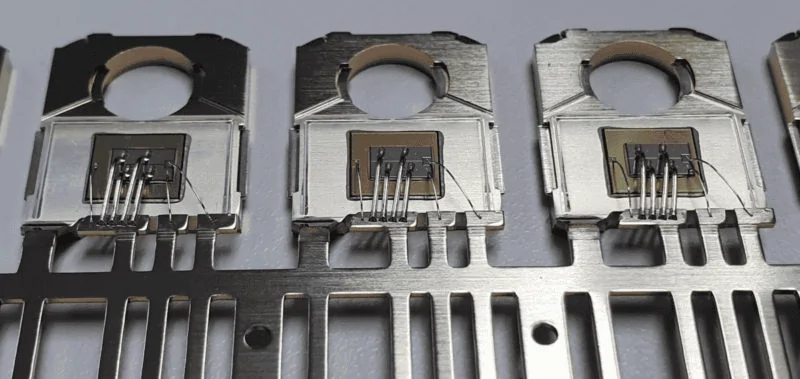
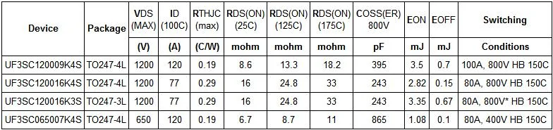
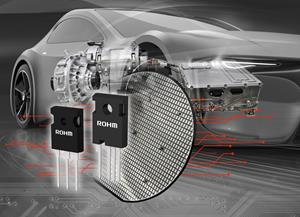
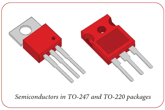
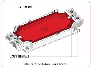
The power semiconductor components most likely to be used in EVs come in two different form factors: (1) plastic types such as the TO-220 and TO-247 packages, which feature wire leads and a (usually non-isolated) heatsink tab, and which typically contain a single diode or switch (with or without anti-parallel diode); (2) modules, which typically contain several components pre-wired in commonly used configurations (e.g. a half-bridge plus a temperature sensor), all mounted on an electrically-isolated heat spreader. Modules also tend to have screw terminals for the high-power connections and pin or spring terminals for the low-power connections, making integration into a bused structure (and replacement of a damaged module) much easier. Despite the radical differences in their physical (and, often, electrical) aspects, there’s no clear distinction for when to choose a plastic package component or a module; using a rather broad brush to delineate between the two, modules are preferred if more than 50-100 A RMS must be handled, whereas plastic packages are preferred if switching frequency must be considerably above the ultrasonic range (e.g. >40 kHz). These are obviously very different criteria, nor are they mutually exclusive, but suffice it to say that if you need to switch >100 A RMS at >100 kHz, then you’re looking at a design challenge worthy of a PhD dissertation.

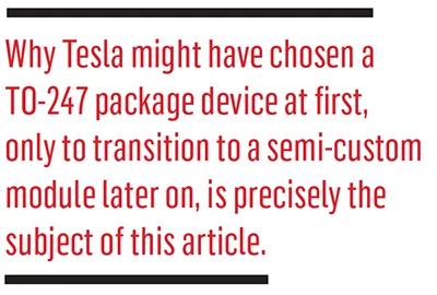
There are numerous other criteria as well as exceptions to the above rules of thumb—for a notable example, Tesla was quite fond of using dozens (84!) of TO-247 switches in its earlier inverters—but it is telling that the Model 3 inverter uses what might be called a quasi-modular approach, with far fewer devices (24) of much higher individual power rating, but still in a plastic package-like form. In fact, why Tesla might have chosen a TO-247 package device at first, only to transition to a semi-custom module later on, is precisely the subject of this article.

Prior to the emergence of OEM EVs, power semiconductor modules were designed specifically for industrial applications, with the vast majority being used in 3-phase motor drives supplied by the AC mains. Consequently, the available voltage ratings were in rather coarse steps of 600 V for 208-240 VAC mains applications, 1,200 V for 440-480 VAC, 1,700 V for 575-600 VAC, and so on. Furthermore, 3-phase motors also come in rather coarse power rating steps, so the current ratings for modules were equally coarse as well. Also, industrial applications tend to be more concerned with reliability and efficiency than with minimizing size (and the noise from “singing” motors and transformers), so the diodes and switches inside the modules weren’t particularly fast (i.e. PWM frequency rarely exceeded 10 kHz, and was usually closer to 1 kHz, especially at 1,200 V and above). Finally, while the market for all industrial motor drives is quite large, the market for any one particular voltage/current combination is relatively small, and some combinations of voltage/current just don’t make sense industrially. For example, it is possible to get 1,700 V modules rated for 3,500 A or higher, but for 600 V modules the highest current rating commonly available is 600 A. This is because no (sane) industrial customer is going to try running a >200 hp motor from 240 V mains!


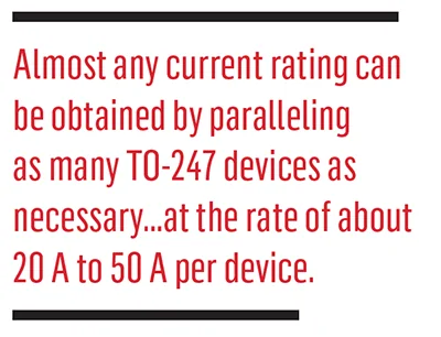
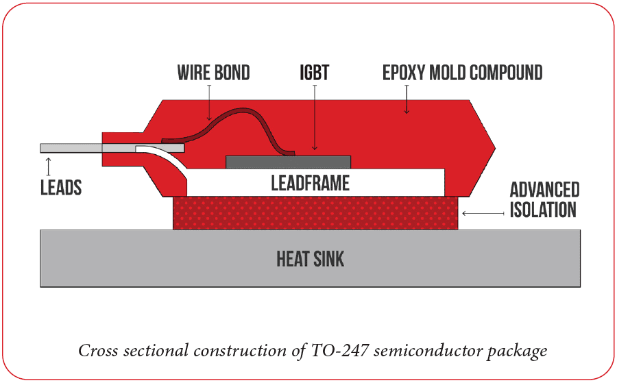
Conversely, there is a veritable smorgasbord of devices and ratings in the plastic TO-247 (and smaller TO-220) packages, such that any practical combination of voltage, current and switching frequency can be had with judicious circuit design and layout (and a PCB capable of handling the current). More specifically, almost any current rating can be obtained by paralleling as many TO-247 devices as necessary…at the rate of about 20 A to 50 A per device, depending on the device technology, total losses, and how heat from said losses is removed from the junction (but note that it takes increasingly heroic measures to keep the junction temperature of a TO-247 device below 100-125° C once dissipation exceeds 50 W). For example, SiC MOSFETs have extremely low switching and conduction losses, and can tolerate operation at much higher temperatures than conventional Si MOSFETs or IGBTs, so the limiting factor on how much current can be crammed through one in a TO-247 package might very well be the ampacity of the bond-wires and/or leads. In contrast, a TO-247 IGBT with a fairly constant voltage drop of 2.2 V and comparatively high switching losses might struggle to handle 25 A, even with liquid cooling. Another factor that greatly affects the ampacity per device is that the heatsink tab on the conventional TO-247 and TO-220 packages is directly connected to the collector or drain, for IGBTs and MOSFETs, respectively, so some form of insulator will be needed between the tab and the heatsink. Unfortunately, most materials which are good electrical insulators are also good thermal insulators, such that even extremely thin sheets of mica, silicone rubber or Kapton (aka polyimide) will add around 1° C/W of thermal resistance to a TO-247 package (and up to 3° C/W for the smaller TO-220). This resistance adds to that of the junction to case and the heatsink to ambient pathways, hence the practical upper limit of 50 W dissipation per TO-247.

There are a couple of exceptions to the “good electrical insulator = poor thermal conductor” rule: aluminum oxide and nitride. The former has a bulk thermal conductivity of 30 W/m-K, while the latter clocks in at 285 W/m-K [see sidebar below: Thermal conductivity vs resistance]. Both compare rather favorably to the thermal conductivity of mica at 0.3 W/m-K (or 100x to almost 1,000x worse), but aluminum nitride is an even better conductor of heat than pure aluminum (235 W/m-K), though still not as good as pure copper (400 W/m-K). Both aluminum oxide and nitride are ceramic-like materials that are hard and brittle, and also like ceramics, they are refractory (i.e. they have a very high melting point), so insulators made from them have to be relatively thick (1 mm seems to be a practical limit) compared to mica (~0.1 to 0.3 mm) or silicone rubber (<0.5 mm). Even so, aluminum oxide and nitride insulators are quite fragile. For example, a product I have helped to redesign utilizes SiC MOSFETs in a TO-247 package with 1 mm-thick aluminum nitride insulators between them and the extruded aluminum heatsink. During UL “open/short” testing (in which the UL inspector randomly opens or shorts various components, looking for potential safety issues), one of the switches exploded and shattered the aluminum nitride insulator. This allowed excessive fault current into earth ground, which is a definite fail of the test (it is perfectly acceptable for your product to quit working during this particular test, it just can’t catch fire or create a shock hazard). Changing the fuse to a faster-acting type (read: more expensive, and more prone to “nuisance trip”) sufficiently limited fault energy to less than what is needed to rupture a TO-247 package, but this is not the sort of thing you want to deal with at the proverbial eleventh hour.


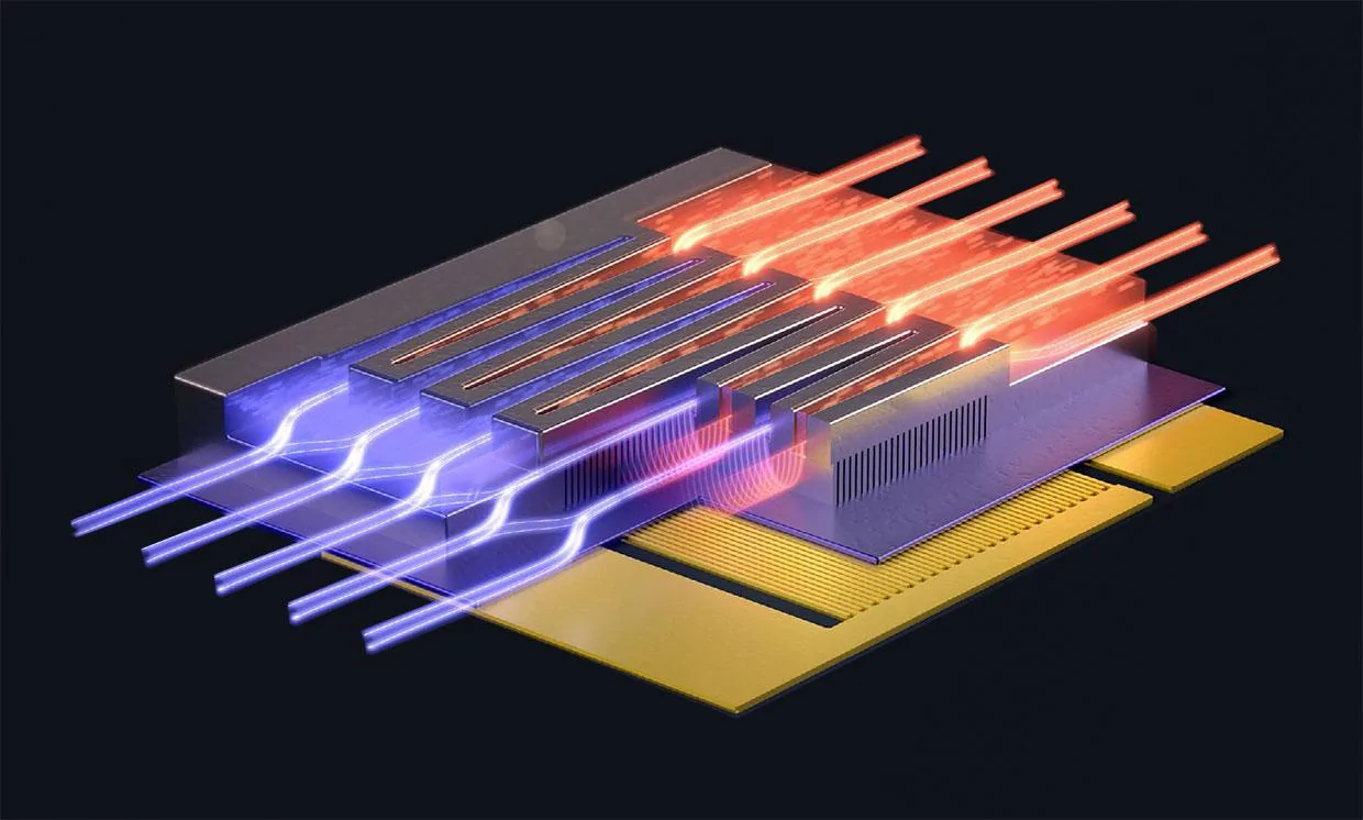
This discussion circuitously segues back to a considerable advantage of modules: the heatsink “tab” is already electrically insulated from the semiconductor dice, and the dice themselves are typically encapsulated in a special silicone gel, which both improves heat removal from the bondwires and does a decent job of containing shrapnel and metal vapor should things go pear-shaped. More specifically, the usual construction of a module is a sandwich consisting of dice soldered to intermediate heat spreaders (usually of copper) to increase the area available for transferring heat (and provide a common electrical connection between dice), followed by an aluminum oxide or nitride sheet which provides electrical isolation and, finally, a single heat spreader which also serves as the mounting baseplate. Basically, the intermediate heat spreaders lower the total thermal resistance from junction to heatsink compared to a solution using multiple TO-247 components, while the silicone gel and aluminum nitride insulators provide considerable voltage withstand rating. In fact, most (if not all) modules for industrial applications have been “recognized” by the major safety agencies (UL, TUV, Intertek, etc) for a given voltage withstand (or “hi-pot”) rating, which makes passing their tests a lot easier (by taking less time and costing less money).

As is usually the case, there are advantages and disadvantages to both types of packaging technology for semiconductors—there’s no such thing as a “one size fits all solution”—and so, unsurprisingly, none of the existing offerings are ideally suited to EV (or hybrid) applications. This is where the advanced packaging solutions conjured up for the Model 3 by Tesla and STMicroelectronics come in: a new approach to module design that combines the low-cost and reduced stray inductance of a plastic package with the electrical isolation, improved thermal performance and greater current rating per device of a classic industrial module, all with a form factor tailored for EV applications, rather than the “one size sort of fits most” of yesterday’s technology.
Sidebar: Thermal conductivity vs resistance
These two specs get tossed around a lot in power electronics, and while thermal resistance is easy to grasp—it is the thermal analog to electrical resistance, with heat in watts as current (okay, that is admittedly confusing) and temperature rise as voltage—thermal conductivity seems to be a bit trickier, mainly because of the confusing units it is given in of W/m-K (or in Imperial units of…on second thought, let’s not even go there). The key difference is that thermal conductivity describes a property of a material in general, while thermal resistance describes a specific use of that material. For example, a 200 mm2 * 1 mm thick insulator pad made of alumina (i.e. aluminum oxide, which has a thermal conductivity of 30 W/m-K) will have a thermal resistance of 0.167° C/W. If the thickness is doubled to 2 mm, then the thermal resistance will also double, while if the area is doubled then the thermal resistance will be halved. In all cases the thermal conductivity is the same, however. Similarly, if the same 200 mm2 * 1 mm insulator is made out of aluminum nitride, then its thermal resistance will plummet to less than 0.018° C/W, or 9.5x less, which makes sense given that aluminum nitride has a thermal conductivity 9.5x better than aluminum oxide.
Source: CHARGED ELECTRIC VEHICLES MAGAZINE
It will interesting to get a glimpse of the PE once it becomes available.
Here is an article on the Model 3 Power Module:
Here’s why Tesla transitioned to a semi-custom power module design in Model 3 inverter
A closer look at semiconductor packaging considerations in EVs
One of the most critical decisions to be made at the earliest stage of designing a new power converter concerns the packages used for the semiconductors, as pretty much every other aspect of the design hinges on their physical form. This is especially true for the main power converters used in EVs—on-board chargers, DC/DC converters and inverters—as there are tight constraints on the size (and cost, of course) allotted to each. Furthermore, any device that has direct or incidental contact with the AC mains will also need to meet some rather onerous electrical safety requirements which—as a case study below will show—can critically depend on the package used for the semiconductor switches.
The power semiconductor components most likely to be used in EVs come in two different form factors: (1) plastic types such as the TO-220 and TO-247 packages, which feature wire leads and a (usually non-isolated) heatsink tab, and which typically contain a single diode or switch (with or without anti-parallel diode); (2) modules, which typically contain several components pre-wired in commonly used configurations (e.g. a half-bridge plus a temperature sensor), all mounted on an electrically-isolated heat spreader. Modules also tend to have screw terminals for the high-power connections and pin or spring terminals for the low-power connections, making integration into a bused structure (and replacement of a damaged module) much easier. Despite the radical differences in their physical (and, often, electrical) aspects, there’s no clear distinction for when to choose a plastic package component or a module; using a rather broad brush to delineate between the two, modules are preferred if more than 50-100 A RMS must be handled, whereas plastic packages are preferred if switching frequency must be considerably above the ultrasonic range (e.g. >40 kHz). These are obviously very different criteria, nor are they mutually exclusive, but suffice it to say that if you need to switch >100 A RMS at >100 kHz, then you’re looking at a design challenge worthy of a PhD dissertation.
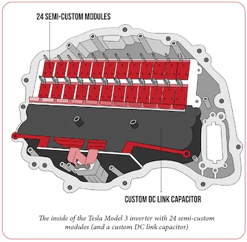
There are numerous other criteria as well as exceptions to the above rules of thumb—for a notable example, Tesla was quite fond of using dozens (84!) of TO-247 switches in its earlier inverters—but it is telling that the Model 3 inverter uses what might be called a quasi-modular approach, with far fewer devices (24) of much higher individual power rating, but still in a plastic package-like form. In fact, why Tesla might have chosen a TO-247 package device at first, only to transition to a semi-custom module later on, is precisely the subject of this article.
Prior to the emergence of OEM EVs, power semiconductor modules were designed specifically for industrial applications, with the vast majority being used in 3-phase motor drives supplied by the AC mains. Consequently, the available voltage ratings were in rather coarse steps of 600 V for 208-240 VAC mains applications, 1,200 V for 440-480 VAC, 1,700 V for 575-600 VAC, and so on. Furthermore, 3-phase motors also come in rather coarse power rating steps, so the current ratings for modules were equally coarse as well. Also, industrial applications tend to be more concerned with reliability and efficiency than with minimizing size (and the noise from “singing” motors and transformers), so the diodes and switches inside the modules weren’t particularly fast (i.e. PWM frequency rarely exceeded 10 kHz, and was usually closer to 1 kHz, especially at 1,200 V and above). Finally, while the market for all industrial motor drives is quite large, the market for any one particular voltage/current combination is relatively small, and some combinations of voltage/current just don’t make sense industrially. For example, it is possible to get 1,700 V modules rated for 3,500 A or higher, but for 600 V modules the highest current rating commonly available is 600 A. This is because no (sane) industrial customer is going to try running a >200 hp motor from 240 V mains!
Conversely, there is a veritable smorgasbord of devices and ratings in the plastic TO-247 (and smaller TO-220) packages, such that any practical combination of voltage, current and switching frequency can be had with judicious circuit design and layout (and a PCB capable of handling the current). More specifically, almost any current rating can be obtained by paralleling as many TO-247 devices as necessary…at the rate of about 20 A to 50 A per device, depending on the device technology, total losses, and how heat from said losses is removed from the junction (but note that it takes increasingly heroic measures to keep the junction temperature of a TO-247 device below 100-125° C once dissipation exceeds 50 W). For example, SiC MOSFETs have extremely low switching and conduction losses, and can tolerate operation at much higher temperatures than conventional Si MOSFETs or IGBTs, so the limiting factor on how much current can be crammed through one in a TO-247 package might very well be the ampacity of the bond-wires and/or leads. In contrast, a TO-247 IGBT with a fairly constant voltage drop of 2.2 V and comparatively high switching losses might struggle to handle 25 A, even with liquid cooling. Another factor that greatly affects the ampacity per device is that the heatsink tab on the conventional TO-247 and TO-220 packages is directly connected to the collector or drain, for IGBTs and MOSFETs, respectively, so some form of insulator will be needed between the tab and the heatsink. Unfortunately, most materials which are good electrical insulators are also good thermal insulators, such that even extremely thin sheets of mica, silicone rubber or Kapton (aka polyimide) will add around 1° C/W of thermal resistance to a TO-247 package (and up to 3° C/W for the smaller TO-220). This resistance adds to that of the junction to case and the heatsink to ambient pathways, hence the practical upper limit of 50 W dissipation per TO-247.
There are a couple of exceptions to the “good electrical insulator = poor thermal conductor” rule: aluminum oxide and nitride. The former has a bulk thermal conductivity of 30 W/m-K, while the latter clocks in at 285 W/m-K [see sidebar below: Thermal conductivity vs resistance]. Both compare rather favorably to the thermal conductivity of mica at 0.3 W/m-K (or 100x to almost 1,000x worse), but aluminum nitride is an even better conductor of heat than pure aluminum (235 W/m-K), though still not as good as pure copper (400 W/m-K). Both aluminum oxide and nitride are ceramic-like materials that are hard and brittle, and also like ceramics, they are refractory (i.e. they have a very high melting point), so insulators made from them have to be relatively thick (1 mm seems to be a practical limit) compared to mica (~0.1 to 0.3 mm) or silicone rubber (<0.5 mm). Even so, aluminum oxide and nitride insulators are quite fragile. For example, a product I have helped to redesign utilizes SiC MOSFETs in a TO-247 package with 1 mm-thick aluminum nitride insulators between them and the extruded aluminum heatsink. During UL “open/short” testing (in which the UL inspector randomly opens or shorts various components, looking for potential safety issues), one of the switches exploded and shattered the aluminum nitride insulator. This allowed excessive fault current into earth ground, which is a definite fail of the test (it is perfectly acceptable for your product to quit working during this particular test, it just can’t catch fire or create a shock hazard). Changing the fuse to a faster-acting type (read: more expensive, and more prone to “nuisance trip”) sufficiently limited fault energy to less than what is needed to rupture a TO-247 package, but this is not the sort of thing you want to deal with at the proverbial eleventh hour.
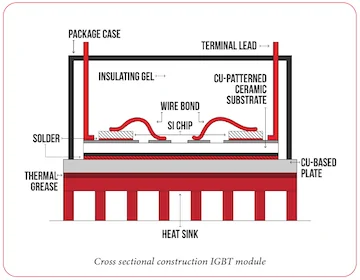
This discussion circuitously segues back to a considerable advantage of modules: the heatsink “tab” is already electrically insulated from the semiconductor dice, and the dice themselves are typically encapsulated in a special silicone gel, which both improves heat removal from the bondwires and does a decent job of containing shrapnel and metal vapor should things go pear-shaped. More specifically, the usual construction of a module is a sandwich consisting of dice soldered to intermediate heat spreaders (usually of copper) to increase the area available for transferring heat (and provide a common electrical connection between dice), followed by an aluminum oxide or nitride sheet which provides electrical isolation and, finally, a single heat spreader which also serves as the mounting baseplate. Basically, the intermediate heat spreaders lower the total thermal resistance from junction to heatsink compared to a solution using multiple TO-247 components, while the silicone gel and aluminum nitride insulators provide considerable voltage withstand rating. In fact, most (if not all) modules for industrial applications have been “recognized” by the major safety agencies (UL, TUV, Intertek, etc) for a given voltage withstand (or “hi-pot”) rating, which makes passing their tests a lot easier (by taking less time and costing less money).
As is usually the case, there are advantages and disadvantages to both types of packaging technology for semiconductors—there’s no such thing as a “one size fits all solution”—and so, unsurprisingly, none of the existing offerings are ideally suited to EV (or hybrid) applications. This is where the advanced packaging solutions conjured up for the Model 3 by Tesla and STMicroelectronics come in: a new approach to module design that combines the low-cost and reduced stray inductance of a plastic package with the electrical isolation, improved thermal performance and greater current rating per device of a classic industrial module, all with a form factor tailored for EV applications, rather than the “one size sort of fits most” of yesterday’s technology.
Sidebar: Thermal conductivity vs resistance
These two specs get tossed around a lot in power electronics, and while thermal resistance is easy to grasp—it is the thermal analog to electrical resistance, with heat in watts as current (okay, that is admittedly confusing) and temperature rise as voltage—thermal conductivity seems to be a bit trickier, mainly because of the confusing units it is given in of W/m-K (or in Imperial units of…on second thought, let’s not even go there). The key difference is that thermal conductivity describes a property of a material in general, while thermal resistance describes a specific use of that material. For example, a 200 mm2 * 1 mm thick insulator pad made of alumina (i.e. aluminum oxide, which has a thermal conductivity of 30 W/m-K) will have a thermal resistance of 0.167° C/W. If the thickness is doubled to 2 mm, then the thermal resistance will also double, while if the area is doubled then the thermal resistance will be halved. In all cases the thermal conductivity is the same, however. Similarly, if the same 200 mm2 * 1 mm insulator is made out of aluminum nitride, then its thermal resistance will plummet to less than 0.018° C/W, or 9.5x less, which makes sense given that aluminum nitride has a thermal conductivity 9.5x better than aluminum oxide.
Source: CHARGED ELECTRIC VEHICLES MAGAZINE
Sponsored
Last edited:
")